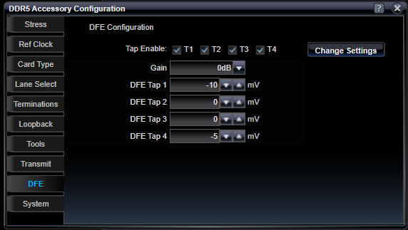
DDR5 DFE Configuration
DDR5 Receivers include a 4-tap Decision Feedback Equalizer (DFE) to improve signal integrity of DDR5 data and command signals in the face of high ISI and crosstalk. DFEs are present in DRAMS as well as in Data Buffers and Register Clocking Devices (RCDs). Depending on the test conditions setup on the Loopback tab, the DDR5 Stress Accessory knows what type of device and can program selected DFE settings over the I2C interface. The source of tap values to use for DFE settings must come from the customer. Typically, these values are learned using DFE simulation analysis or in oscilloscope emulation functions. Estimates for DFE values can also be made by looking a losses present in Deferred Eye diagrams.
Negative gain values typically imply a high-pass filter. The Tap value for tap N refers to how much DC offset will be added (or subtracted) from the received signal N UI's of registered bit delay. See the DDR5 Specification for more detailed information on DFE.

|
Tap Enable |
|
|
T1 / T2 / T3 / T4 |
Individual enables for each of the four taps of DFE |
|
Gain |
|
|
-6dB / -4dB / -2dB / 0dB / 2dB / 4dB / 6dB |
Before DFE processing is done, the received Rx signal can have its amplitude adjusted by -6 dB to +6 dB in 2 dB increments. Small input signals can be gained up and large input signals can be attenuated down. Many test applications simply leave this setting at 0 dB. |
|
DFE Tap 1 / 2 / 3 / 4 |
|
|
mV |
Signed number of millivolts (in 5 mV increments) to be added or subtracted to received signal on UI boundaries. |
|
Change Settings |
|
|
|
Once all settings are configured, this command will actually initiate the I2C communication to the test device to configure the DFE. |
Running DFE Tap Operations
Setting DFE Taps takes a few seconds to complete. During this time, progress messages and ending status are provided on the Command Log tab.
See Also