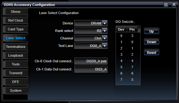
DDR5 Lane Select Configuration
The DDR5 test application depends
|
Device |
|
|
DRAM, RCD, DB |
Selects the type of device being tested. This selection modifies what test lanes are presented below. DB is only available if test card type is an LRDIMM. See Test Card type in Card Type Configuration. |
|
Rank Select |
|
|
R0 / Rank0 / Rank1 |
If multiple ranks are present, you can select which rank to use for testing. Data lanes of different ranks can share DQ/DQS settings (and, therefore, SMP connectors on the CTC2 board) and the chip select is used to communicate individually between them. |
|
Channel |
|
|
ChA / ChB |
DDR5 supports two nearly independent memory channels on each module. Tests can be done on either channel by making this selection. |
|
Test Lane |
|
|
DQ00_A - DQ31_A / DQ00_B - DQ31_B / CA0_A - CA6_A / CA0_B - CA6_B |
Tests lanes can be either data lanes or CA (command address) lanes on either the A-side or the B-side of the DRAM. The Combo test card pre-defines only a few types of test lanes, while the LRDIMM and RDIMM offer the full complement of test lanes. Choose a lane here and then connect DQ and DQS wires (as instructed) to enable testing for the specific lane. If the test lane is on a DRAM and happens to land on bit0 of that DRAM, then only the DQ and DQS wiring is needed. However, if a non-zero bit in a DRAM is to be tested, then an extra connection from the general purpose open-collector outputs on the Stress Accessory will also be needed to be connected to the bit0 of the DRAM to be tested, just to be able to set up I2C communication to that DRAM for testing. |
|
PG Clock Out Connects to |
|
|
|
The SMP connector name on the CTC2 board or, in general, the DDR5 common name for the clocking pair needed to be connected to the Pattern Generator Ch0+/Ch0- signals to complete the test, as defined by above settings. |
|
PG Data Out Connects to |
|
|
|
The SMP connector name on the CTC2 board or, in general, the DDR5 common name for the data wire needed to be connected to the Pattern Generator Ch1+ signals to complete the test, as defined by above settings. |
|
DQ Swizzle |
|
|
|
Test Lanes are specified in terms of the lanes referred to inside the DDR5 DRAM registers. These internal lanes may not be connected to the DDR5 connector lanes in a 1:1 fashion, so a "Swizzle" mapping is provided for associating DDR5 DRAM register lanes to DDR5 connector lanes associated with the CTC2 Breakout board. This mapping is used, for example, to indicate which signals the PG should connect to on the CTC2 board. |
See Also